 |
|
Silicon @ Fermilab: Past and Future by Kurt Riesselmann
In the 1970s, the discovery of two heavy quarks, charm and bottom, began a new era of particle physics with unprecedented technological demands. Produced in high-energy collisions, heavy quarks decay within a tiny fraction of a second, traveling less than a few centimeters from their point of production.
To study properties like the lifetime and decays of these new particles, physicists needed compact, high-precision detectors to closely monitor the interaction point where particle beams create these unstable forms of matter. Thin slices of silicon, which produce an electrical impulse when charged particles fly across them, had become available, and physicists began exploring silicon's detection capabilities.
"The first silicon detectors were developed in the late 1970s," said Jeff Spalding, who took part in Fermilab experiment E691, the first Fermilab particle physics experiment to implement semi-conducting microstrip detectors. Its use of silicon detectors followed the R&D work carried out by European particle physicists in Munich, Germany and Geneva, Switzerland. Experimenters soon realized that silicon detectors would revolutionize the field by allowing for exploration of matter in greater detail.
"Silicon detectors offer extremely high spatial resolution," explained Spalding. "They opened a whole new realm of physics and precision measurements."
Placing layers of silicon sensors as close as possible to the interaction point is crucial to identifying particle tracks that originate from either charm or bottom quark decays. Tracing the signals caused by decay products back to their origin, scientists can determine the location of a particle's decay to secondary particles and calculate, for example, particle masses and lifetimes.
In the early 1990s, the CDF collaboration installed the first silicon detector in a colliding-beam experiment at Fermilab. To surround the almost two-foot-long interaction region with silicon sensors, physicists reduced the size of readout electronics and place it inside the space in which they also wanted to track
particles. Using integrated chips, small electronic devices that amplify and transmit the signals created inside the silicon, scientists managed to solve the problem.
"It was clear that we needed a much larger facility to build these major upgrades," recalled Spalding. "In 1992, Lenny Spiegel and I went to the director and explained the need for a facility with large clean rooms and appropriate equipment."
The idea for Fermilab's Silicon Detector facility was born. The Research Division (now Particle Physics) identified four old experimental halls, which at that time received more visits from birds and raccoons than from physicists, to host the new facility. Spiegel was responsible for revitalizing the buildings and setting up the SiDet facility.
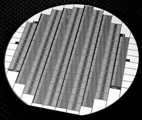
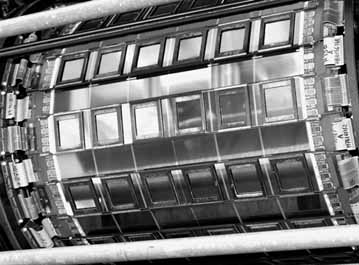
Today, more than 6000 square feet of clean room with dozens of high-precision machines are dedicated to probe, mount and connect silicon strips; to outfit them with electronic chips; and to assemble all components into a compact structure that can be installed at the center of a state-of-the-art particle experiment.
"In our field, there is no other comparable facility," said Joe Incandela, the head of the facility. "We have the most space, the most machines. We can carry out each step necessary in the assembly of silicon detectors, and we can produce large volumes."
The true secret of the success, however, is the people working at the SiDet facility.
"The strength of SiDet is the cohesiveness of the people working here," said Spiegel, who is associate leader at the facility. "At peak times, about 100 people worked at SiDet: technicians, engineers, physicists, many visiting scientists from around the world. Their skills and knowledge have formed the basis for building the new silicon detectors for CDF and DZero."
"We see a huge workload in the future," said Spiegel. He just ordered the first of two robots, developed at the European particle physics laboratory CERN, that will be used in mounting large quantities of CMS silicon strip wafers on support structures. Starting in 2001, SiDet workers will assemble about half of the 2500 square feet of silicon for the CMS detector. The rest is split among several European facilities.
In addition to silicon strips, the CMS experiment will also use new pixel technology. Instead of dividing silicon wafers in narrow bands of 50-micron width and several inches long, the new silicon wafers feature small rectangular-shaped areas of 150 by 150 microns. A single layer of silicon pixels provides more detailed information on where a particle traversed the panel.
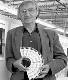
"Presently, we have about 10 people working on the prototyping of the forward pixel detector," said Bruno Gobbi, professor at Northwestern University. He is part of the U.S.-CMS collaboration that is, among other projects, responsible for the design and construction of four 12-inch silicon pixel disks that will record particles leaving the collision area in the forward direction.
SiDet's greatest challenge may come from Fermilab's future BTeV experiment, which will use the Tevatron beams to measure differences between properties of bottom quarks and antiquarks. If physicists obtain final funding, the experiment will begin operation in 2006.
"For the BTeV experiment, we expect the silicon pixel detector to have 31 million readout channels," said Simon Kwan, a physicist working on the BTeV pixel R&D program. "We aim at placing our silicon detectors closer to the Tevatron beams than any other experiment." At a distance of six millimeters, the detector will be more than twice as close as the CDF and DZero silicon detectors. The BTeV collaboration plans to be the first experiment to have silicon detectors in vacuum, separated from the primary beam only by a thin shield.
Placing silicon detectors close to the collision area puts enormous demands on the design of silicon devices, the supporting mechanical structures and the electronic readout equipment. All pieces, for example, must withstand high levels of energy transfer. Cooperating with research institutes around the world, Fermilab physicists are able to gather the necessary information about material properties.
The R&D efforts for both CMS and BTeV silicon detectors are centered at Fermilab's Silicon Microdetector laboratory, led by Greg Sellberg. Located inside the SiDet buildings, the lab provides the high-tech equipment for physicists to develop and test new silicon detector technologies.
"It is a juggling act if you have three projects going on at the same time," said Sellberg. "But you have to keep the users happy."
Preparing for future experiments, Sellberg and his colleagues will have many balls in the air in the years ahead. |
 In their quest to explore the microcosm, physicists have employed increasingly sophisticated tools to track particles, measure their energy and identify their decays. As they discovered twelve fundamental components of matter, the quarks and leptons, they met the challenge and created devices that differentiate among the variety of elementary particles produced in their experiments.
 The success of CDF's first silicon detector, called SVX, encouraged physicists to design more sophisticated silicon devices and upgrade both the CDF and DZero detectors for Run II, set to begin in March 2001. They envisioned using the SVX technology on a much larger scale. Instead of the original 43,000 readout channels, a measure for the number of independent silicon strips, both CDF and DZero physicists made plans for silicon detectors with about 800,000 readout channels.
 Right now the SiDet facility is entering a transition period as it prepares for future tasks. The increased collision rate of the Tevatron collider will reduce the lifetime of the new silicon detectors, and physicists hope to replace them in 2004. In addition, Fermilab has agreed to construct one quarter of the silicon modules for the CMS experiment, scheduled to begin taking data in 2006 at the new Large Hadron Collider in Europe.
| last modified 12/1/2000 email Fermilab |
FRLsDFx9eyfrPXgV